

March 10, 2026 (Source) — Homerun Resources Inc. (TSXV: HMR) (OTCQB: HMRFF) (“Homerun” or the “Company”) is pleased to announce that researchers at the University of California, Davis (“UC Davis”), in collaboration with Homerun, have successfully produced fused silica glass from raw silica sand using a one-step thermoelectric Fast Joule Heating (“FJH”) process. These tests demonstrate, at bench scale, that silica from Homerun’s Santa Maria Eterna (SME) Silica Sand Project can be converted directly into fused silica glass without chemical reagents, supporting the Company’s strategy to supply high-value advanced materials markets.
Building upon the prior test work completed by independent materials consultancy Dorfner Anzaplan (see news release), which confirmed that the raw SME silica sand is suitable as feedstock for fused silica production using conventional multi-step processing methods, Homerun and UC Davis specifically set out to evaluate whether that same material could be processed to fused silica glass using new, more efficient one-step thermoelectric processing techniques. The UC Davis testing has now produced fused silica glass.
The issue confronting wider adoption of high-purity fused silica across high volume traditional and novel end-uses is the limited supply and high price due to the cost of conventional processing techniques.

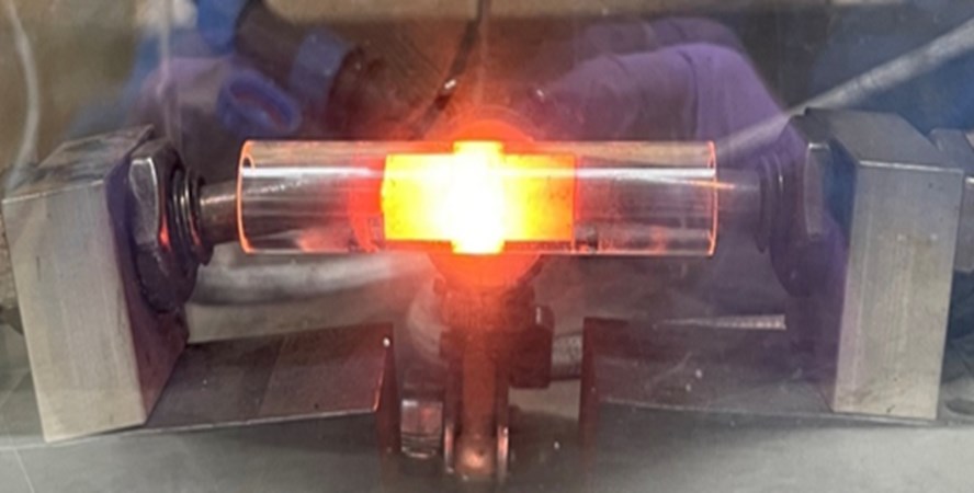
Figure 1. Image of the flash-joule heating process and setup. A conductive material (here carbon black) is sandwiched between graphite plugs and undergo a rapid heating process as a charged voltage is released from the capacitor. This entire setup is enclosed within a vacuum-sealed chamber, which can be purged and filled with various gases to enable controlled atmospheric environments.
To view an enhanced version of this graphic, please visit:
https://images.newsfilecorp.com/files/4082/287929_657bcb83d4b91916_001full.jpg
Subhash Risbud, Director of the Risbud Research Group at UC Davis, stated, “Critical to the success of our FJH process was incorporating a conductive medium for the current to flow while yet keeping the silica powder separated. Thus, we developed a new tube-within-tube configuration in which silica is confined to the inner tube while the outer tube contains the conductive substrate (graphite). This approach helps sustain the high temperatures required for extended processing. Based on our results, the silica to fused silica glass synthesis has worked using our FJH equipment (as shown in Figure 1). Fused silica glass was achieved very rapidly after our processing peak temperature reached about 2000 C (above the 1710 C melting point of silica). These exciting new results in processing to fused silica glass using Flash Joule Heating are reported as part of the continuing collaborative research being conducted by the Risbud Research Group at UC Davis and adds to previous new laser-based techniques developed in the same lab for the purification of the SME silica sand, all under the continuing funding from Homerun.”
“Utilizing the Fast Joule Heating method to process a raw silica sample from the Homerun SME Silica Sand Project into fused silica glass is a big step in our advanced materials development,” stated Brian Leeners, CEO of Homerun. “The FJH method does not use any chemical reagents and therefore generates no polluting waste stream. If the energy source is renewable, then this is a completely green process. We chose FJH for this testing as it has been scaled utilizing off-the-shelf equipment in other critical materials processing. These techniques, after the necessary improvements, can produce fused silica glass used for medical, pharmaceutical, electronics, photonics and other similar technology and energy applications.”
The next step in the Homerun / UC Davis testing plan is to incorporate off-the-shelf equipment to begin scaling the production capacity of the fused silica glass using FJH. This testing was initiated immediately after the successful bench testing.
Fused silica tech markets are dominated by semiconductor fabrication, high-performance optics, and advanced electronics, driven by its extreme purity, thermal stability, and optical clarity. Key applications include lithography lenses, wafer substrates, fiber optics, and laser systems, with growing demand from 5G, IoT, and long-term data storage. Ultra-pure fused silica also serves as a high-performance, low-loss substrate for superconducting qubits and as a base material for silicon-based, spin-qubit quantum computers.
Nvidia recently announced a combined investment of US$4 billion into two photonics companies, Lumentum and Coherent to advance photonics technology for AI data centers. The multiyear agreements include purchase commitments and capacity access for advanced optical networking products, supporting U.S.-based manufacturing and R&D. The move targets performance and efficiency gains in AI systems by enhancing data transfer capabilities using photonics.
Photonics uses light instead of electrical signals through copper, enabling faster and more energy-efficient data transfer. Nvidia’s adoption of co-packaged optics in Spectrum and Quantum switches removes the need for pluggable modules on the switch side, cutting hardware requirements and power consumption. This technology is essential for connecting multiple AI systems or data centers over extended distances. Nvidia success could lead to direct integration of photonics into Nvidia’s GPUs, boosting AI training speed and efficiency. Alternatively, faster innovation from competitors such as Amazon or Google could challenge Nvidia’s position. Control over photonics supply might also lengthen lead times for rivals, reshaping the competitive dynamics in the optics market.
https://www.cnbc.com/2026/03/02/nvidia-investment-coherent-lumentum.html
“NVIDIA is advancing the world’s most sophisticated silicon photonics to build the next generation of gigawatt-scale AI factories.”
NEW PATENT APPLICATION ADDED TO PATENT PORTFOLIO
Homerun also announces that a new patent application has been filed for an invention resulting under the Company’s partnership with UC Davis. The invention relates to a:
“PROCESS FOR OBTAINING HIGH-PURITY SILICA SAND AND THE RESULTING PRODUCT.”
The invention describes a novel, environmentally friendly process for purifying silica sand to ultra-high purity levels, primarily targeting industrial applications such as semiconductors, LCDs, and optical glass. The process leverages femtosecond laser ablation, which eliminates the need for hazardous chemicals and energy-intensive mechanical methods traditionally used in silica purification.
Key Steps in the Process: Grinding, Vacuum, Laser Treatment and analysis.
Results and Advantages:
- Purity Improvement: The analysis shows a significant reduction in impurities (Ti, Ca, Mg, Fe), with purity increasing from 99.75% to +99.99%.
- Environmental Benefits: The process avoids hazardous chemicals and reduces energy consumption compared to conventional methods.
- Industrial Relevance: The resulting high-purity quartz silica sand (HPQ) is suitable for demanding industrial uses.
The above UC Davis fused silica glass testing results have not been independently verified and may also be the subject of a future Homerun Patent Application.

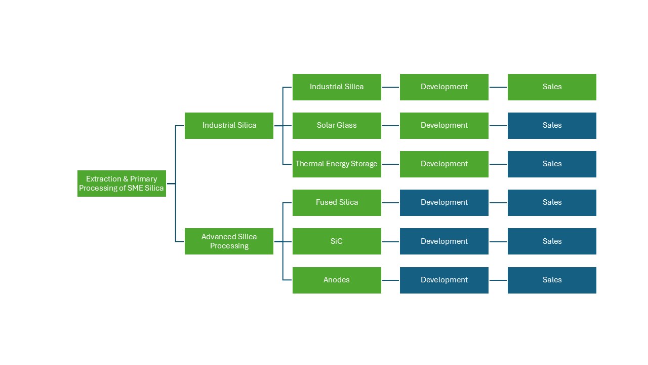
Figure 2. Homerun’s silica value chain from extraction to advanced products, highlighting development and sales across each segment.
To view an enhanced version of this graphic, please visit:
https://images.newsfilecorp.com/files/4082/287929_657bcb83d4b91916_002full.jpg
About Homerun
Homerun is building the silica-powered backbone of the energy transition across four focused verticals: Silica, Solar, Energy Storage, and Energy Solutions. Anchored by a unique high-purity low-iron silica resource in Bahia, Brazil, Homerun transforms raw silica into essential products and technologies that accelerate clean power adoption and deliver durable shareholder value.
- Silica: Secure supply and processing of high-purity low-iron silica for mission-critical applications, enabling premium solar glass and advanced energy materials.
- Solar: Development of Latin America’s first dedicated 1,000 tonne per day high-efficiency solar glass plant and the commercialization of antimony-free solar glass designed for next-generation photovoltaic performance.
- Energy Storage: Advancement of long-duration, silica-based thermal storage systems and related technologies to decarbonize industrial heat and unlock grid flexibility.
- Energy Solutions: AI-enabled energy management, control systems, and turnkey electrification solutions that reduce costs and optimize renewable generation for commercial and industrial customers.
With disciplined execution, strategic partnerships, and an unwavering commitment to best-in-class ESG practices, Homerun is focused on converting milestones into markets – creating a scalable, vertically integrated platform for clean energy manufacturing in the Americas.
On behalf of the Board of Directors of
Homerun Resources Inc.
“Brian Leeners”
Brian Leeners, CEO & Director
[email protected] / +1 604-862-4184 (WhatsApp)
Tyler Muir, Investor Relations
[email protected] / +1 306-690-8886 (WhatsApp)
FOR THE ADEQUACY OR ACCURACY OF THIS RELEASE
The information contained herein contains “forward-looking statements” within the meaning of applicable securities legislation. Forward-looking statements relate to information that is based on assumptions of management, forecasts of future results, and estimates of amounts not yet determinable. Any statements that express predictions, expectations, beliefs, plans, projections, objectives, assumptions or future events or performance are not statements of historical fact and may be “forward-looking statements”.
Neither the TSX Venture Exchange nor its Regulation Services Provider (as that term is defined in policies of the TSX Venture Exchange) accepts responsibility for the adequacy or accuracy of this release.


Leave a Reply